Tatyana Gotsulenko
BIM Case Studies
June 3, 2025
Optimizing Semiconductor Plant Design with BIM: Lessons from Intel FAB38
The global demand for semiconductors continues to surge, driving the need for more efficient, precise, and scalable manufacturing environments. Designing a semiconductor plant is one of the most technically challenging tasks in industrial construction – where even the smallest design error can lead to massive financial losses or production delays.
At BIM Leaders LTD, we’ve seen firsthand how Building Information Modeling (BIM) transforms the planning and construction of semiconductor facilities into a more intelligent, coordinated, and data-driven process. A powerful case study of this is the design and construction of Intel’s Fab38 – a benchmark for semiconductor plant design efficiency and innovation.
Why Semiconductor Facilities Demand a BIM Approach
 Source: techtime.news
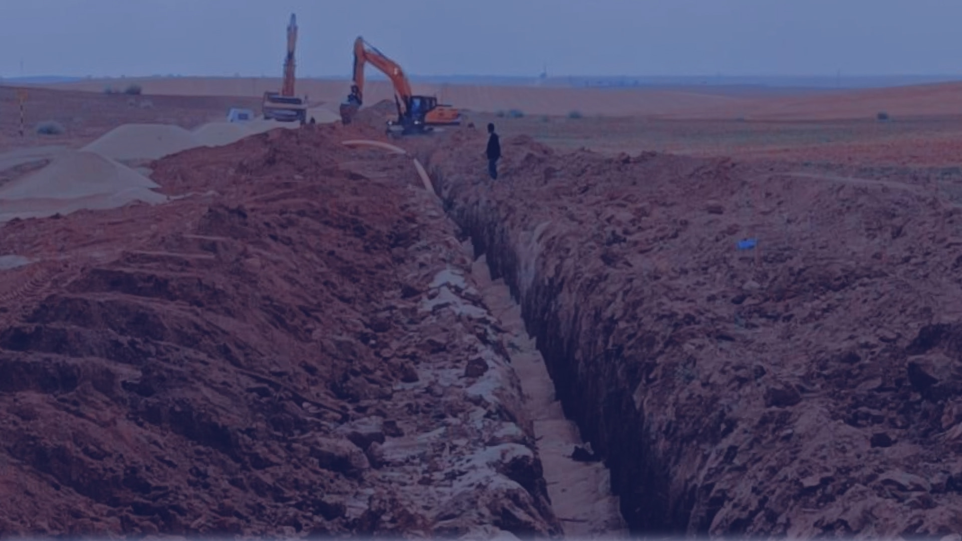
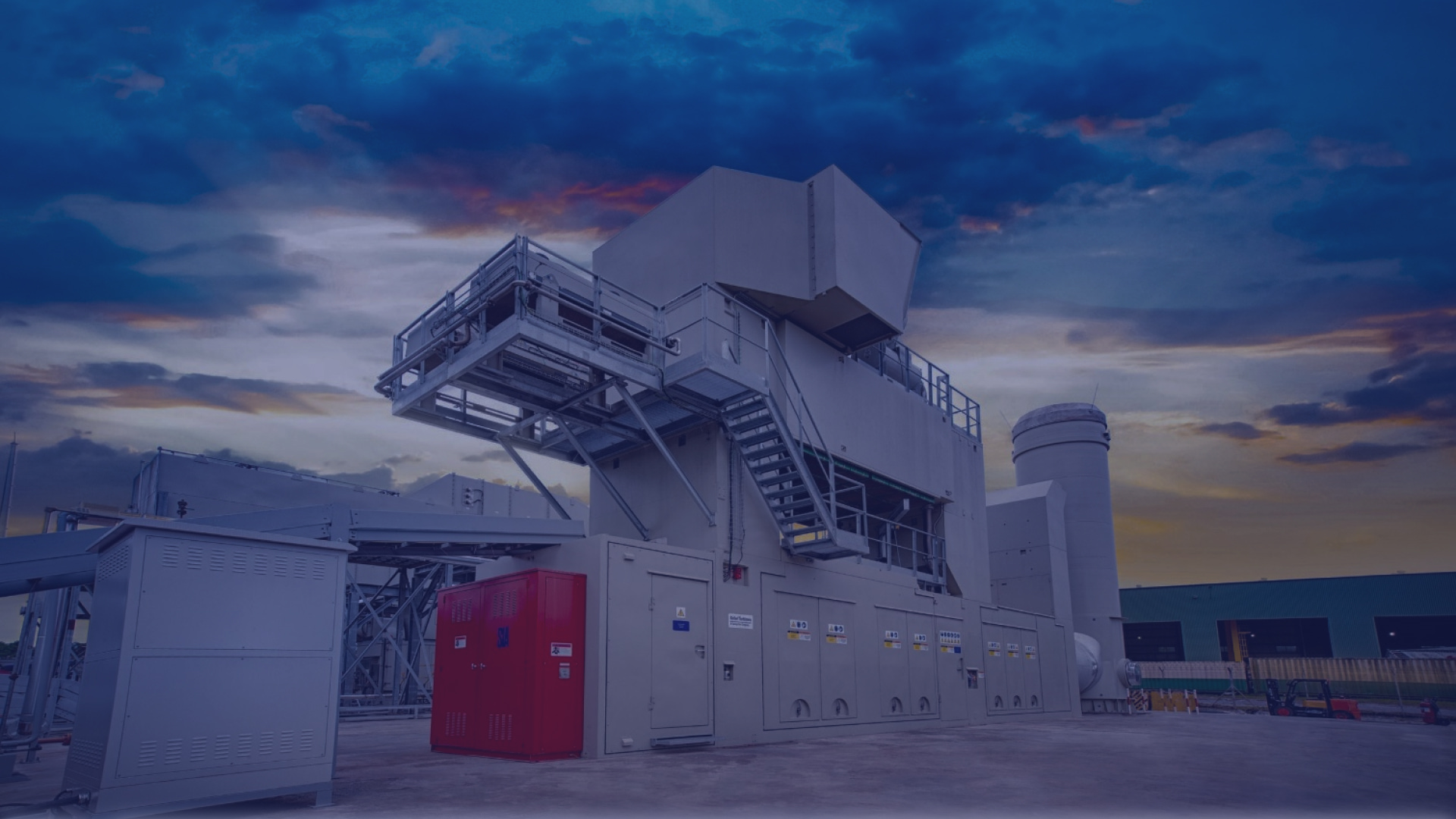
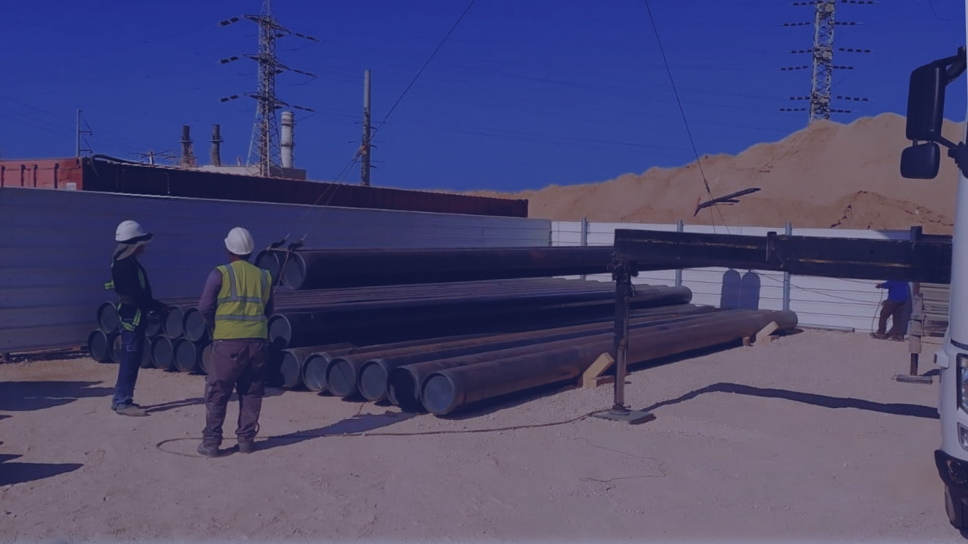
As semiconductor manufacturing becomes more complex, precision is non-negotiable. Facilities like FAB38 must house thousands of multi-million-dollar machines, connected by hundreds of kilometers of piping, cabling, and support systems. Any miscalculation could delay launch dates and inflate costs dramatically.
Traditional design approaches often include “buffer zones” to mitigate risk – but these add significant, often unnecessary, costs. BIM enables designers to eliminate guesswork and instead build a highly accurate digital model that optimizes space, systems, and resource use from day one.
Accuracy and Clash Detection
With BIM, all systems – from HVAC to water supply – are modeled digitally before construction begins.
Clash detection tools help identify and resolve conflicts early in the design phase, long before they become costly on-site issues.
Clash detection tools help identify and resolve conflicts early in the design phase, long before they become costly on-site issues.
Real-Time Coordination Across Disciplines
A central, cloud-based BIM model enables architects, engineers, project managers, and contractors to collaborate in real time. Everyone works from the same data set, minimizing miscommunication and improving alignment across disciplines.
Cost and Schedule Optimization (4D/5D BIM)
With 4D (time) and 5D (cost) integration, teams can simulate construction schedules and adjust project timelines dynamically. This real-time insight enables cost forecasting and ensures that semiconductor plants like FAB38 are built on time and within budget.
Laser Scanning and BIM As-Built Models
For retrofitting or facility upgrades, laser scanning captures the exact geometry of existing environments. These scans feed directly into BIM to create precise as-built models, which are essential for ensuring alignment between new designs and real-world conditions.
Design Verification and Augmented Reality
BIM data can be paired with AR tools to assist on-site technicians. Imagine a technician replacing a pipe in a live semiconductor plant — with AR glasses, they can visualize the entire facility layout in real time, avoiding disruptions and reducing downtime.
Future-Proofing Through BIM
BIM is more than a construction tool – it is a foundation for long-term operational excellence. Whether planning an expansion, integrating new tech, or performing routine maintenance, BIM ensures that future upgrades are fast, safe, and cost-effective.
Conclusion: BIM Is the Future of Semiconductor Plant Design
In a world where precision, speed, and cost-efficiency define success in semiconductor manufacturing, BIM offers a strategic edge. From digital twins to modular design and automated workflows, this technology is reshaping how we plan, build, and operate semiconductor factories.
At BIM Leaders LTD, we bring unmatched expertise in designing complex technical infrastructure – from cleanrooms and control centers to full-scale manufacturing plants. We ensure that every detail aligns with global industry standards and every project phase is executed with world-class accuracy.
At BIM Leaders LTD, we bring unmatched expertise in designing complex technical infrastructure – from cleanrooms and control centers to full-scale manufacturing plants. We ensure that every detail aligns with global industry standards and every project phase is executed with world-class accuracy.
Ready to build the next generation of semiconductor facilities?
Let’s design the future together.
Explore our experience: Our case studies
Explore our experience: Our case studies